- 您现在的位置:买卖IC网 > Sheet目录2005 > LTC1856IG#PBF (Linear Technology)IC ADC 16BIT 100KSPS 28-SSOP
2
LTC1854/LTC1855/LTC1856
185456fa
Consult LTC Marketing for parts specified with wider operating temperature ranges.
1
2
3
4
5
6
7
8
9
10
11
12
13
14
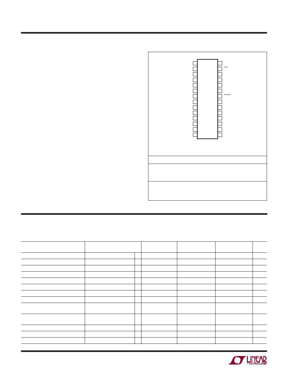
TOP VIEW
G PACKAGE
28-LEAD PLASTIC SSOP
28
27
26
25
24
23
22
21
20
19
18
17
16
15
COM
CH0
CH1
CH2
CH3
CH4
CH5
CH6
CH7
MUXOUT+
MUXOUT–
ADC+
ADC–
AGND1
CONVST
RD
SCK
SDI
DGND
SDO
BUSY
OVDD
DVDD
AVDD
AGND3
AGND2
REFCOMP
VREF
A
U
G
W
A
W
U
W
A
R
BSOLUTEXI
TI
S
Supply Voltage (OVDD = DVDD = AVDD = VDD) ........... 6V
Ground Voltage Difference
DGND, AGND1, AGND2, AGND3 ......................
±0.3V
Analog Input Voltage
ADC+, ADC–
(Note 3) ...................(AGND1 – 0.3V) to (AVDD + 0.3V)
CH0-CH7, COM ..................................................
±30V
Digital Input Voltage (Note 4) ...... (DGND – 0.3V) to 10V
Digital Output Voltage .... (DGND – 0.3V) to (DVDD + 0.3V)
Power Dissipation .............................................. 500mW
Operating Temperature Range
LTC1854C/LTC1855C/LTC1856C ............ 0
∞C to 70∞C
LTC1854I/LTC1855I/LTC1856I .......... – 40
∞C to 85∞C
Storage Temperature Range ................. – 65
∞C to 150∞C
Lead Temperature (Soldering, 10 sec) ................. 300
∞C
TJMAX = 110
∞C, qJA = 95∞C/W
(Notes 1, 2)
ORDER PART NUMBER
LTC1855CG
LTC1855IG
PACKAGE/ORDER I FOR ATIO
UU
W
The
● denotes the specifications which apply over the full operating temperature range, otherwise specifications are at TA = 25
∞C.
MUXOUT connected to ADC inputs. (Notes 5, 6)
CO VERTER A D
ULTIPLEXER CHARACTERISTICS
U
W
U
Order Options Tape and Reel: Add #TR
Lead Free: Add #PBF
Lead Free Tape and Reel: Add #TRPBF
Lead Free Part Marking: http://www.linear.com/leadfree/
LTC1854CG
LTC1854IG
LTC1856CG
LTC1856IG
LTC1854
LTC1855
LTC1856
PARAMETER
CONDITIONS
MIN
TYP
MAX
MIN
TYP
MAX
MIN
TYP
MAX
UNITS
Resolution
●
12
14
16
Bits
No Missing Codes
●
12
14
15
Bits
Transition Noise
0.06
0.25
1
LSBRMS
Integral Linearity Error
(Note 7)
●
±1
±1.5
±3LSB
Differential Linearity Error
●
–1
1
–1
1.5
–2
4
LSB
Bipolar Zero Error
(Note 8)
●
±5
±8
±23
LSB
Bipolar Zero Error Drift
±0.1
ppm/
∞C
Bipolar Zero Error Match
3
4
10
LSB
Bipolar Full-Scale Error
External Reference (Note 11)
●
±0.34
±0.14
±0.1
%
Internal Reference (Note 11)
±0.45
±0.40
±0.4
%
Bipolar Full-Scale Error Drift
External Reference
±2.5
ppm/
∞C
Internal Reference
±7
ppm/
∞C
Bipolar Full-Scale Error Match
5
10
15
LSB
Input Common Mode Range
●
±10
V
Input Common Mode Rejection Ratio
96
dB
发布紧急采购,3分钟左右您将得到回复。
相关PDF资料
LTC1859IG#TRPBF
IC A/D CONV 8CH 16BIT 28-SSOP
LTC1867AIGN#TRPBF
IC ADC 16BIT 8CH 200KSPS 16SSOP
LTC1867LCGN#PBF
IC ADC 16BIT 8CH 175KSPS 16SSOP
LTC2142IUP-14#PBF
IC ADC DUAL 14BIT 65MSPS 64QFN
LTC2143CUP-14#PBF
IC ADC DUAL 14BIT 80 MSPS 64-QFN
LTC2153IUJ-14#PBF
IC ADC 14BIT DUAL 310MSPS 40QFN
LTC2158IUP-14#TRPBF
IC ADC DUAL 14BIT 310M 64-QFN
LTC2172IUKG-14#TRPBF
IC ADC 14BIT SER/PAR 65M 52-QFN
相关代理商/技术参数
LTC1856IG#TRPBF
功能描述:IC ADC 16BIT 100KSPS 28-SSOP RoHS:是 类别:集成电路 (IC) >> 数据采集 - 模数转换器 系列:- 标准包装:1,000 系列:- 位数:12 采样率(每秒):300k 数据接口:并联 转换器数目:1 功率耗散(最大):75mW 电压电源:单电源 工作温度:0°C ~ 70°C 安装类型:表面贴装 封装/外壳:24-SOIC(0.295",7.50mm 宽) 供应商设备封装:24-SOIC 包装:带卷 (TR) 输入数目和类型:1 个单端,单极;1 个单端,双极
LTC1857CG
制造商:Linear Technology 功能描述:ADC Single SAR 100ksps 12-bit Serial 28-Pin SSOP
LTC1857CG#PBF
功能描述:IC ADC 8CH 12BIT 100KSPS 28-SSOP RoHS:是 类别:集成电路 (IC) >> 数据采集 - 模数转换器 系列:SoftSpan™ 标准包装:1 系列:microPOWER™ 位数:8 采样率(每秒):1M 数据接口:串行,SPI? 转换器数目:1 功率耗散(最大):- 电压电源:模拟和数字 工作温度:-40°C ~ 125°C 安装类型:表面贴装 封装/外壳:24-VFQFN 裸露焊盘 供应商设备封装:24-VQFN 裸露焊盘(4x4) 包装:Digi-Reel® 输入数目和类型:8 个单端,单极 产品目录页面:892 (CN2011-ZH PDF) 其它名称:296-25851-6
LTC1857CG#PBF
制造商:Linear Technology 功能描述:ADC, 8CH, 12BIT, 100KSPS, SSOP-28
LTC1857CG#TRPBF
功能描述:IC A/D CONV 8CH 12BIT 28-SSOP RoHS:是 类别:集成电路 (IC) >> 数据采集 - 模数转换器 系列:SoftSpan™ 标准包装:1,000 系列:- 位数:12 采样率(每秒):300k 数据接口:并联 转换器数目:1 功率耗散(最大):75mW 电压电源:单电源 工作温度:0°C ~ 70°C 安装类型:表面贴装 封装/外壳:24-SOIC(0.295",7.50mm 宽) 供应商设备封装:24-SOIC 包装:带卷 (TR) 输入数目和类型:1 个单端,单极;1 个单端,双极
LTC1857CGPBF
制造商:Linear Technology 功能描述:ADC,LTC1857 12bit 100kSPS 8 ch SPI SSOP
LTC1857IG
制造商:Linear Technology 功能描述:MS-ADC/General Purpose, 12-bit, 100ksps, 8-ch. SoftSpan ADC
LTC1857IG#PBF
功能描述:IC A/D CONV 8CH 12BIT 28-SSOP RoHS:是 类别:集成电路 (IC) >> 数据采集 - 模数转换器 系列:SoftSpan™ 标准包装:1,000 系列:- 位数:12 采样率(每秒):300k 数据接口:并联 转换器数目:1 功率耗散(最大):75mW 电压电源:单电源 工作温度:0°C ~ 70°C 安装类型:表面贴装 封装/外壳:24-SOIC(0.295",7.50mm 宽) 供应商设备封装:24-SOIC 包装:带卷 (TR) 输入数目和类型:1 个单端,单极;1 个单端,双极